
URL: https://www.desy.de/news/news_search/index_eng.html
Breadcrumb Navigation
DESY News: Filming the film: Scientists observe photographic exposure live at the nanoscale
News
News from the DESY research centre
Filming the film: Scientists observe photographic exposure live at the nanoscale
Photoinduced chemical reactions are responsible for many fundamental processes and technologies, from energy conversion in nature to micro fabrication by photo-lithography. One process that is known from everyday’s life and can be observed by the naked eye, is the exposure of photographic film. At DESY's X-ray light source PETRA III, scientists have now monitored the chemical processes during a photographic exposure at the level of individual nanoscale grains in real-time. The advanced experimental method enables the investigation of a broad variety of chemical and physical processes in materials with millisecond temporal resolution, ranging from phase transitions to crystal growth. The research team lead by Prof. Jianwei (John) Miao from the University of California in Los Angeles (UCLA) and Prof. Tim Salditt from the University of Göttingen report their technique and observations in the journal Nature Materials.

The X-rays were not only used to expose the photographic paper, but also to analyse changes of its inner composition at the same time. The paper carries a photosensitive film of a few micrometre thickness, consisting of tiny silver bromide grains dispersed in a gelatine matrix, and with an average size of about 700 nanometres. A nanometre is a millionth of a millimetre. When X-rays impinge onto such a crystalline grain, they are diffracted in a characteristic way, forming a unique pattern on the detector that reveals properties like crystal lattice spacing, chemical composition and orientation. “We could observe individual silver bromide grains within the ‘burn’ paper since the X-ray beam had a size of only 270 by 370 nanometres – smaller than the average grain,” says Salditt, who is a partner of DESY in the construction and operation of the GINIX (Göttingen Instrument for Nano-Imaging with X-Rays) at beamline P10.
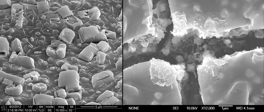
The phozographic paper before (left) and after (right) exposure seen through a scanning electron microscope. Credit: Jeff (Zhifeng) Huang/UCLA
“As advanced synchrotron light sources are currently under rapid development in the US, Europe and Asia,” the authors anticipate that “in situ X-ray nanodiffraction, which enables to measure atomic resolution diffraction patterns with several millisecond temporal resolution, can be broadly applied to investigate phase transitions, chemical reactions, crystal growth, grain boundary dynamics, lattice expansion, and contraction in materials science, nanoscience, physics, and chemistry.”
Reference
Grain rotation and lattice deformation during photoinduced chemical reactions revealed by in situ X-ray nanodiffraction; Zhifeng Huang, Matthias Bartels, Rui Xu, Markus Osterhoff, Sebastian Kalbfleisch, Michael Sprung, Akihiro Suzuki, Yukio Takahashi, Thomas N. Blanton, Tim Salditt und Jianwei Miao; Nature Materials, 2015; DOI: 10.1038/NMAT4311
Video1.mov
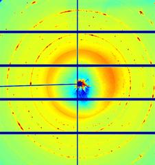
The X-ray diffraction pattern reveals the dynamic changes within the photo sensitive film during exposure, as individual diffraction peaks move and split up. Credit: Jeff (Zhifeng) Huang/UCLA
