URL: https://www.desy.de/news/news_search/index_eng.html
Breadcrumb Navigation
DESY News: Nanostructures assemble themselves
News
News from the DESY research centre
Nanostructures assemble themselves
Research scientists at DESY have developed a new procedure that allows metallic nanostructures to simultaneously assemble and line up all by themselves. This so-called bottom-up approach offers a quick and simple alternative to existing procedures, making it interesting for commercial applications, too, in which nanostructures are used more and more often. “Most importantly, the method allows extremely uniform nanostructures to be created in highly regular patterns with comparatively little effort,” explains Denise Erb from the DESY research group of Ralf Röhlsberger. A special set-up, developed by group member Kai Schlage, allowed the scientists to actually watch the nanostructures as they grew with DESY’s X-ray source PETRA III. The three scientists are presenting the method and its first results in the journal Science Advances.

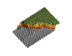
Composition of the nanostructure: On the approximately 10 nanometres (nm) deep grooves of an aluminium oxide (grey) a 40nm thick layer of copolymers (brown) is deposited, internally forming chemical domains. On suitable domains, metal nanodots (green) grow. Here, they reached a height of about 10nm. The area shown measures 3000nm by 1800nm. Credit: Denise Erb, DESY
Nanostructures are turning up more and more often in everyday life. “Nanostructures permit improved or new functionalities. In catalytic converters, for example, data storage devices or sensors,” says Erb. “The dimensions of the products we normally deal with in our everyday lives are generally of the order of a few centimetres or more. So it would be nice to be able to manufacture materials that incorporate nanostructures on that scale too. And ideally they should be quick and cheap to make, as well.” However, it is often very challenging to create nanostructures both on large surfaces and with the necessary regularity. This is where the new method comes into its own.
The conventional top-down technique can be compared with sculpting: one begins with a smooth surface and gradually carves out the desired pattern. This is done bit by bit, which means that the manufacturing time depends on the size of the required area. The advantage is that virtually any desired pattern can be created.
The method used by the researchers at DESY, on the other hand, is based on the so-called bottom-up approach. This makes use of the fact that certain materials have a natural tendency to form nanostructures. “In bottom-up methods, which are also known as self-organising methods, we do not force the material to adopt a certain pattern, as in the top-down method,” explains Erb. “Instead, we create conditions that allow the material to self-assemble and form nanostructures. The shape of these nanostructures cannot be chosen arbitrarily, as in top-down procedures – they are dictated by the properties of the material. Nonetheless, the nanostructures that form are extremely interesting to us, and useful.” The big advantage is that the nanostructures form over the entire surface at the same time, so that the speed with which the pattern is formed no longer depends on the size of the surface.

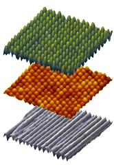
The copolymer layer (brown) self-assembles onto the grooved crystal surface (grey). Within the copolymer chemical domains form with one type of domain rising about 2 nanometres (nm) above the other, forming regular hills. On these hills metal nanodots grow (green). The area shown measures about 1000nm by 1000 nm. Credit: Denise Erb, DESY
A crystal of aluminium oxide serves as the base. When this is heated to above 1000 degrees Celsius, nanometre-scale grooves form on the previously smooth crystal surface – which now resembles a nano-washboard. The next layer is now put down on this first nanostructured pattern. It consists of a film of so-called copolymers. Polymers are long-chain molecules, and copolymers are made up of several different types of polymers. The copolymer used by the scientists contains the same polymers as those found in Perspex or polystyrene. In the copolymer, however, the polymers are linked to each other differently, which leads to different properties in the resulting material.
“The copolymer chains have two chemically different ends which do not get along with each other: similar ends can get close together, opposite ends cannot. This is why the molecules in the copolymer film arrange themselves in so-called domains,” explains Erb. “The grooved crystal does not affect the copolymer via chemical bonds but much more straightforwardly: the chains of molecules, and hence also the domains, are of a fixed size, so they only fit on the nanostructured crystal in a certain way. And the best fit is reached when the nanometre small domains within the copolymer accurately follow the crystal grooves.” As a result, the arrangement of the nanostructures (grooves) on the surface of the crystal dictates the arrangement of the nanostructures (domains) in the copolymer film.
The final step consists of creating small hummocks of metal atoms on the surface of the copolymer film, so-called nanodots. Nanodots made of iron are the crucial culminating feature of the entire structure, because the researchers at DESY are particularly interested in the magnetic behaviour of nanostructures, for example to contribute to the development of better magnetic data storage. Here they can exploit the different chemical properties of the copolymer domains, which interact with metals to different degrees. “First, a metal vapour is created that precipitates onto the copolymer surface. If a metal atom encounters a domain with which it experiences a strong chemical interaction, it clings to it. Conversely the metal atom will not adhere to domains with which it only experiences a weak interaction,” explains Erb. In this way, mounds of iron atoms form on the surface of the copolymer, with valleys in the areas where no iron atoms adhere. The result is the required array of magnetic nanostructures.

Furthermore, the dimensions of the metal nanodots can be influenced by changing external conditions, such as the temperature. The higher the temperature, the more mobile the metal atoms become. Sluggish metal atoms can only form flat, broad nanostructures; highly mobile metal atoms, on the other hand, can form tall, narrow nanostructures.

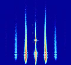
Example of an X-ray scattering pattern of a growing nanostructure, recorded at beamline P01 at PETRA III. Credit: Kai Schlage, DESY
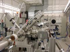
With the help of the x-ray beam, scientists can see, for example, how the shape and the magnetic properties of the nanostructures evolve. Not only can they examine the results of their efforts, but also study the intermediate stages in more detail. As in football, the scientists are not simply interested in the final outcome of the game, but also on how it came about. They would like to know, for example, which parameters played a key role. “Through our research, we hope to establish a method by which nanostructures can be created more easily and quickly,” concludes Erb, “but also to develop a better understanding of why these tiny structures behave magnetically, chemically and optically the way they do.”
Reference:
„Uniform metal nanostructures with long-range order via 3-step hierarchical self-assembly“; D. J. Erb, K. Schlage, R. Röhlsberger; „Science Advances“, 2015; DOI: 10.1126/sciadv.1500751


