URL: https://www.desy.de/news/news_search/index_eng.html
Breadcrumb Navigation
DESY News: Hot aluminum etches smooth nano-holes in semiconductors
News
News from the DESY research centre
Hot aluminum etches smooth nano-holes in semiconductors
A German-French research team has identified surprising properties of nano-holes in semiconductor materials produced by a promising technique: In their experiments, hot aluminum droplets have etched remarkable smooth holes in an aluminum gallium arsenide (AlGaAs) substrate. The method is suitable, among other things, for the production of so-called quantum dots, which can be used, for example, for light sources with a very sharply defined color or for storage cells in quantum computers. The team from the Center for Hybrid Nanostructures (CHyN) at the University of Hamburg, the DESY NanoLab and the European Synchrotron Radiation Source (ESRF) in Grenoble, France, present their findings in the journal Physical Review Materials.

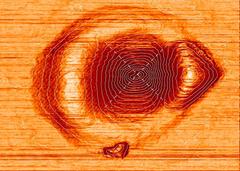
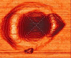
A single nano hole under the atomic force microscope AFM at CHyN. The contour lines indicate the mostly even slope of smooth walls. Credit: CHyN

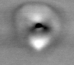
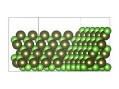
For their etching experiments, the researchers coated the semiconductor material with aluminum, which forms droplets on the surface. At temperatures of nearly 700 degrees Celsius, the aluminum droplets etched holes into the semiconductor material. “Surprisingly, at temperatures above 665 degrees Celsius, holes with a smooth and angular shape, like a pointed, angular funnel, were formed,” reports Vonk. “That was unexpected, because when etching, one actually imagines 'fringed' structures. But the aluminum obviously etches smooth holes.” The smooth, regular shape of the holes became visible during X-ray examinations at the ESRF. Why the hot aluminum leads to these regular shapes is not yet fully understood and is probably due to the thermodynamic properties of the materials used.
Investigations with an atomic force microscope at CHyN and with a scanning electron microscope at the DESY Nanolab showed that the holes are each about 100 nanometres wide and 60 nanometres deep. One nanometre is one millionth of a millimetre. Other metals can also be used in the process, but the dependence of the shape and facets on the material still needs to be clarified. Such holes could serve as templates for quantum dots with tailor-made properties by being filled with a new material. The researchers now hope to find out how the shape of the nano-holes can be understood and controlled in futures analyses.
Reference :
Faceting of Local Droplet-etched Nanoholes in AlGaAs; Vedran Vonk, Taras Slobodskyy, Thomas F. Keller, Marie-Ingrid Richard, Sara Fernández, Tobias Schulli, Christian Heyn, Wolfgang Hansen und Andreas Stierle; Physical Review Materials, 2018; DOI: 10.1103/PhysRevMaterials.2.106001


